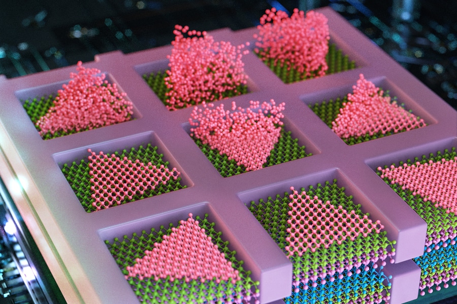
MIT engineers have innovated a novel method to fabricate sturdy 3D chips without the need for bulky silicon wafers. This advancement promises to significantly enhance computing power, fueling next-generation AI, memory and logic devices.
In an industry-defining breakthrough, MIT engineers have unveiled a groundbreaking new approach to semiconductor design. By developing a novel method to construct high-rise, multilayered 3D chips without the need for traditional silicon wafer substrates, this innovation could radically amplify the efficiency and capability of future electronic devices.
Traditionally, the number of transistors on a chip has increased by making them smaller and packing them tightly on a single surface. But as physical and technological limits are reached, the industry is turning to vertical stacking — envisioning chips much like high-rise buildings instead of sprawling ranch houses. These multi-layer chips have the potential to exponentially increase data handling and processing capabilities.
Jeehwan Kim, a study author and an associate professor of mechanical engineering at MIT, calls this breakthrough a game changer.
“This breakthrough opens up enormous potential for the semiconductor industry, allowing chips to be stacked without traditional limitations,” he said in a news release. “This could lead to orders-of-magnitude improvements in computing power for applications in AI, logic, and memory.”
Published in the journal Nature, the study details how this approach was realized.
The MIT team, in collaboration with Samsung Advanced Institute of Technology, Sungkyunkwan University in South Korea and the University of Texas at Dallas, successfully fabricated these multilayered chips using high-quality semiconducting materials stacked directly on top of one another. Their method circumvents the need for thick, bulky silicon wafers, making room for more direct and efficient communication between layers.

Credit: Cube 3D Graphic
Kim’s team had previously achieved significant progress in growing high-quality semiconducting materials on amorphous surfaces, which are part of the diverse topography of completed chips. These materials, known as transition-metal dichalcogenides (TMDs), maintain their properties even at atomic-scale dimensions, unlike silicon, whose performance degrades significantly at smaller scales.
In earlier experiments, the team grew TMDs on silicon wafers with tiny, pattern-creating pockets. These pockets served as “seeds” where atoms settled and grew in a single-crystalline pattern. The challenge, however, was doing so at high temperatures which would damage the underlying circuitry.
“You have to grow this single-crystalline material below 400 Celsius; otherwise, the underlying circuitry is completely cooked and ruined,” Kim added.
To overcome this, the team adapted a concept from metallurgy. They discovered that nucleation — the initial phase of crystal formation — occurs more effectively at the mold’s edges, a process which requires less energy and lower temperatures. Leveraging this concept, they placed TMD seeds at the edges of the pockets, facilitating the growth of single-crystalline material at a much lower 380 degrees Celsius.
The breakthrough didn’t stop there. The researchers also successfully stacked alternating layers of different TMDs (molybdenum disulfide for n-type transistors, and tungsten diselenide for p-type transistors) on top of each other directly.
This method effectively doubles the density of a chip’s semiconducting elements, greatly enhancing its computational prowess.
“A product realized by our technique is not only a 3D logic chip but also 3D memory and their combinations,” Kim added.
First author Kiseok Kim, a postdoctoral associate in Jeehwan Kim‘s lab, emphasizes the advantages over traditional 3D chips with silicon wafers.
“Conventional 3D chips have been fabricated with silicon wafers in-between, by drilling holes through the wafer — a process which limits the number of stacked layers, vertical alignment resolution, and yields,” he said in the news release. “Our growth-based method addresses all of those issues at once.”
Jeehwan Kim recently founded FS2 (Future Semiconductor 2D materials) to commercialize this innovative approach.
“We so far show a concept at a small-scale device arrays. The next step is scaling up to show professional AI chip operation,” he added.
Supported by the Samsung Advanced Institute of Technology and the Air Force Office of Scientific Research, this breakthrough by MIT pioneers sets the stage for the development of AI hardware that rivals today’s supercomputers, integrated into everyday devices from laptops to wearables.

